Insight
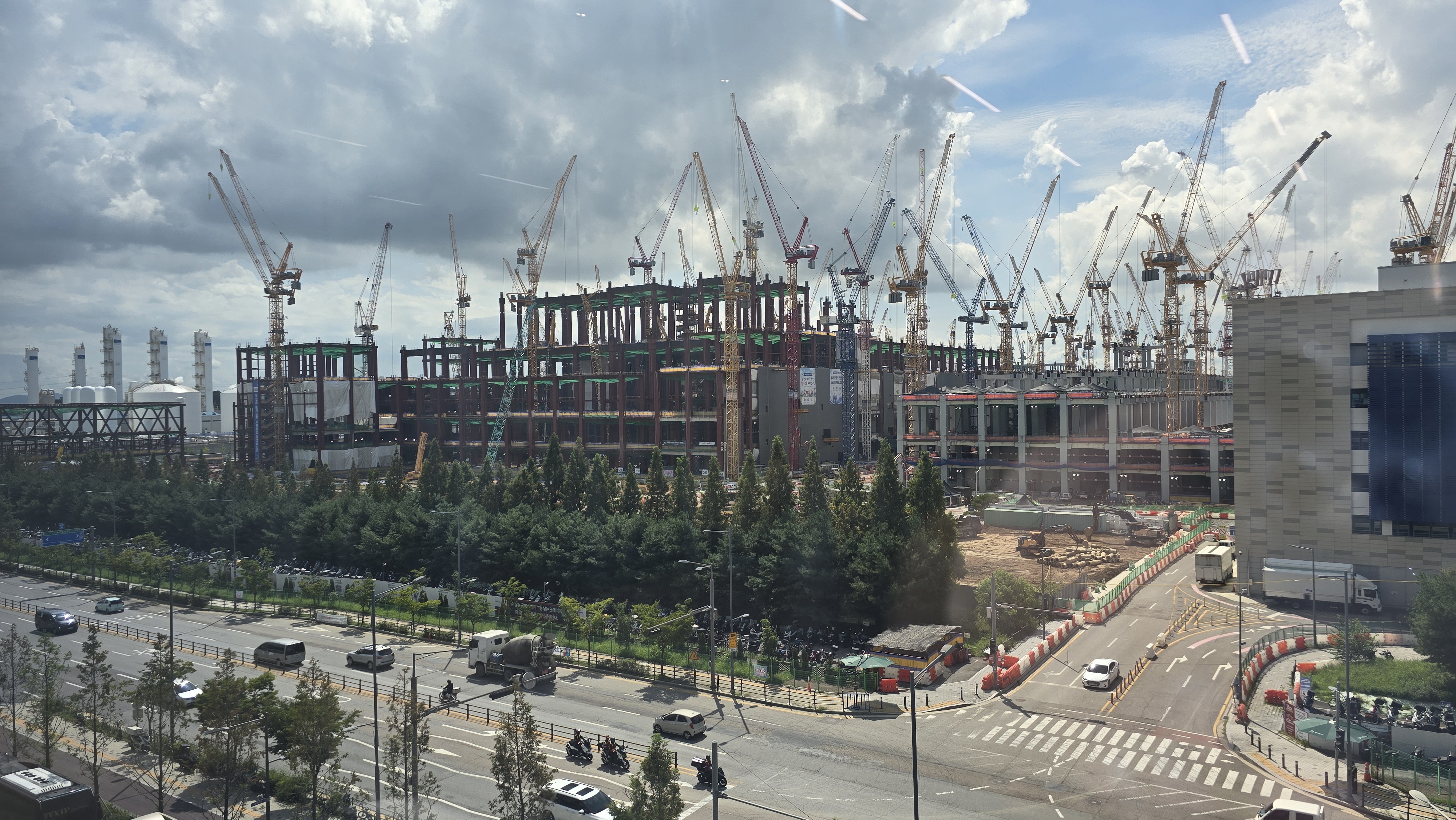
Inside Samsung’s Semiconductor Fab Strategy: How Pyeongtaek P1–P6 Are Built, Operated and Expanded
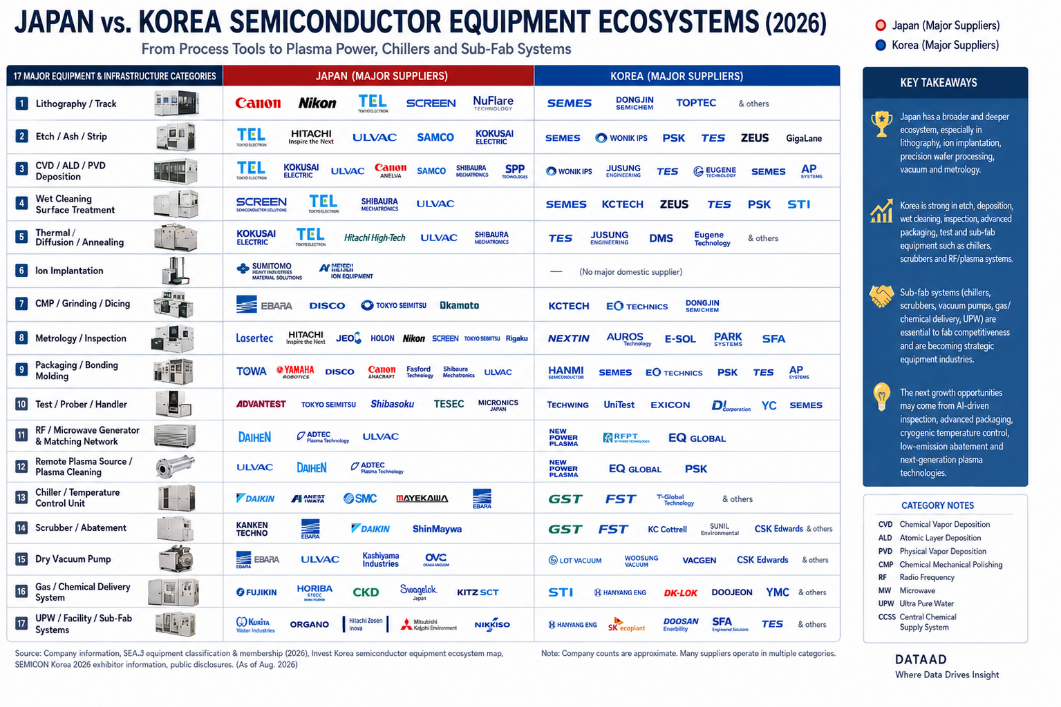
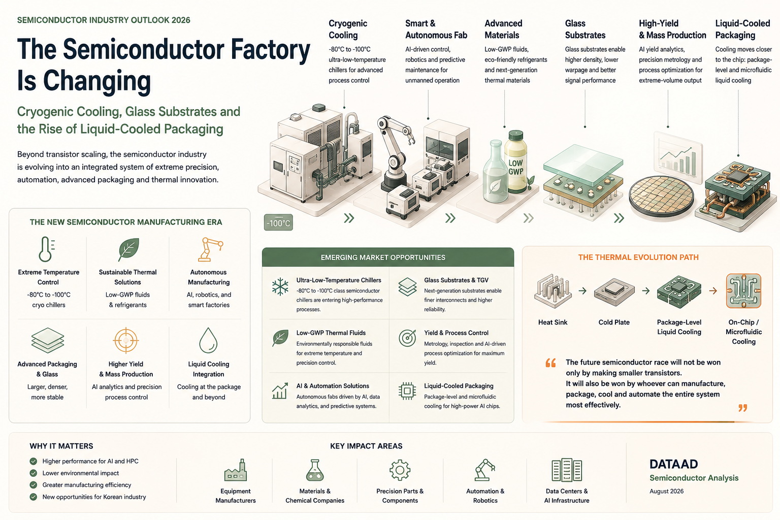
Samsung’s Pyeongtaek campus shows how a modern semiconductor fab is built as a vertically integrated manufacturing system combining cleanrooms, utilities, vacuum systems, abatement, HBM production and advanced packaging. With P5 and P6 accelerating and new fabs planned in Yongin and Gwangju, Korea is entering another major semiconductor infrastructure cycle.