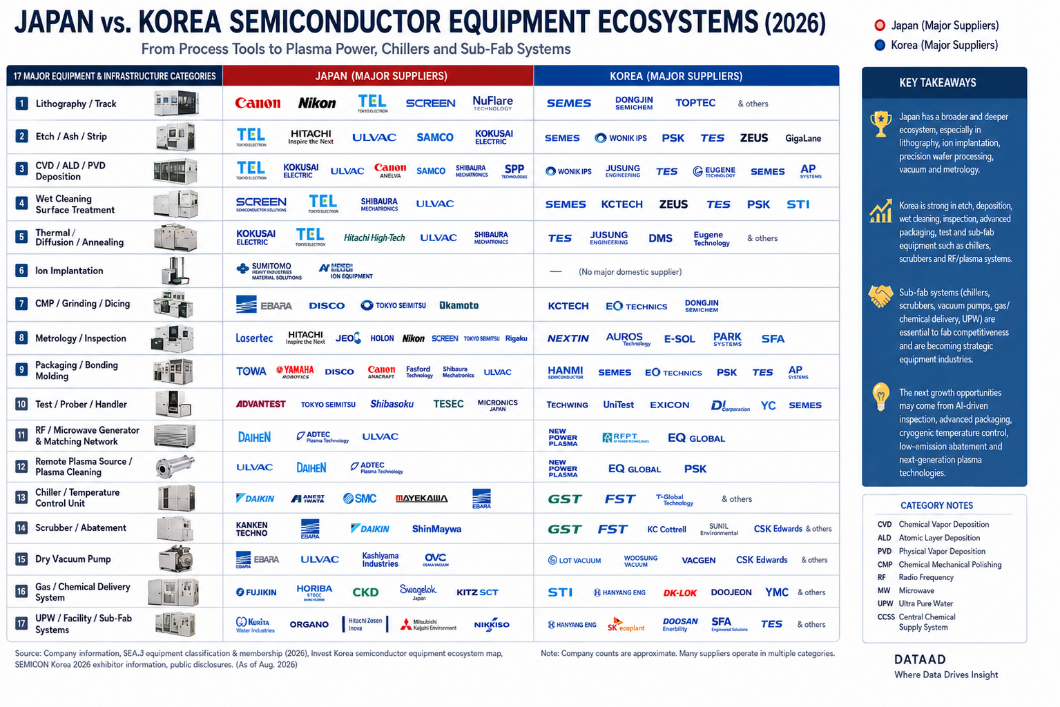
A Semiconductor Fab Is Much More Than a Collection of Process Tools
When people discuss semiconductor manufacturing equipment, the conversation usually begins with lithography, etching and deposition.
But a semiconductor fabrication plant cannot operate with those machines alone.
Every process chamber depends on a much larger ecosystem of RF power generators, impedance matching networks, remote plasma sources, vacuum pumps, chillers, scrubbers, gas delivery systems, chemical supply equipment, ultrapure water and other facility infrastructure.
In many cases, these supporting systems operate continuously below or beside the main production floor.
They may be less visible than an exposure scanner or etcher, but they are equally essential to semiconductor yield, safety, uptime and productivity.
For this reason, DATAAD expanded its Korea-Japan semiconductor equipment comparison from conventional process tools to 17 major equipment and infrastructure categories.
How DATAAD Counts the Equipment Ecosystem
There is no single official database that provides an exact number of semiconductor equipment manufacturers by process in Korea and Japan.
Many companies operate in several categories, while hundreds of smaller companies manufacture components, modules, subsystems or customized equipment.
The figures below therefore represent a DATAAD editorial mapping of major domestic-headquartered manufacturers with identifiable commercial semiconductor equipment or subsystem product lines.
A company may appear in more than one category.
| Equipment Category | Japan | Korea | Relative Position |
|---|---|---|---|
| 1. Lithography / Track | Approx. 5–6 major makers | Approx. 2–3 | Japan Strong |
| 2. Etch / Ash / Strip | Approx. 5–6 | Approx. 6–7 | Korea Competitive |
| 3. CVD / ALD / PVD Deposition | Approx. 7+ | Approx. 6–7 | Both Strong |
| 4. Wet Cleaning / Surface Treatment | Approx. 4–5 | Approx. 4–5 | Both Competitive |
| 5. Thermal / Diffusion / Annealing | Approx. 4–5 | Approx. 3–4 | Japan Broader |
| 6. Ion Implantation | 2 major specialists | Very Limited | Japan Strong Advantage |
| 7. CMP / Grinding / Dicing | Approx. 4–5 | Approx. 2–3 | Japan Strong |
| 8. Metrology / Inspection | Approx. 8+ | Approx. 5–6 | Japan Broader, Korea Rising |
| 9. Packaging / Bonding / Molding | Approx. 7–8 | Approx. 5–7 | Both Strong |
| 10. Test / Prober / Handler | Approx. 5+ | Approx. 5–6 | Both Competitive |
| 11. RF / Microwave Generator & Matching | Approx. 3+ major specialists | Approx. 3+ major specialists | Both Technically Strong |
| 12. Remote Plasma Source / Plasma Cleaning | Several specialists | Approx. 2–3 strong specialists | Korea Has Strategic Capability |
| 13. Chiller / Temperature Control Unit | Several specialist suppliers | Approx. 3+ major suppliers | Korea Strong |
| 14. Scrubber / Gas Abatement | Approx. 3–4 major suppliers | Approx. 3+ major suppliers | Both Strong |
| 15. Dry Vacuum Pump | Approx. 4+ major suppliers | Approx. 1–2 major domestic specialists | Japan Strong |
| 16. Gas / Chemical Delivery | Approx. 5+ major equipment and component suppliers | Approx. 3–5 major system suppliers | Both Competitive |
| 17. UPW / Facility / Sub-Fab Systems | Multiple global-scale suppliers | Multiple engineering and utility suppliers | Japan Broader, Korea Strong Locally |
Note: These figures are an editorial ecosystem map rather than a statutory company census. Suppliers operating across multiple categories are counted in each relevant segment.
1. Lithography: Japan Still Holds a Major Structural Advantage
Lithography remains one of the clearest differences between Japan and Korea.
Japan is home to Canon and Nikon, two of the very few companies globally capable of manufacturing semiconductor exposure systems.
Tokyo Electron and SCREEN also have major positions in resist coating and development equipment, while NuFlare Technology is strategically important in electron-beam mask writing.
Korea has developed photo-track and supporting process technologies through companies such as SEMES and other domestic suppliers, but it does not yet have a domestic equivalent of ASML, Canon or Nikon for leading wafer exposure.
2–3. Etching and Deposition: Korea Has Built Real Depth
Etching and deposition show a very different picture.
Japan has Tokyo Electron, KOKUSAI ELECTRIC, ULVAC, Canon Anelva, SAMCO and other highly specialized process-equipment companies.
Korea has built a substantial equipment ecosystem around Samsung Electronics and SK hynix.
Representative Korean companies include SEMES, WONIK IPS, JUSUNG Engineering, TES, Eugene Technology, PSK, ZEUS and GigaLane.
This is where proximity to large memory fabs creates an enormous strategic advantage.
Equipment companies can develop new processes together with major customers, qualify components locally and improve tools through repeated production feedback.
4–5. Cleaning and Thermal Processing
Japan remains particularly strong in wafer cleaning through SCREEN, while Tokyo Electron and several specialist manufacturers participate across cleaning and surface preparation.
Korea also has meaningful domestic capability through companies such as ZEUS, KC Tech, PSK, TES and STI.
Thermal processing is another established Japanese field, particularly through companies with long histories in furnaces, oxidation, diffusion and batch processing.
Korea has fewer internationally visible suppliers, but domestic companies continue to expand their presence around memory-related thermal processes.
6. Ion Implantation Remains a Major Korean Gap
Ion implantation remains one of Korea’s clearest equipment weaknesses.
Japan has specialized manufacturers capable of supplying high-current, medium-current and high-energy implantation systems.
Korea has yet to establish an equivalent domestic supplier with significant global semiconductor production volume.
This category demonstrates why semiconductor manufacturing capacity and semiconductor equipment self-sufficiency are very different measurements.
7. CMP, Grinding and Dicing: Japan’s Precision Machinery Heritage
Japan has extraordinary depth in wafer processing.
EBARA is a major CMP equipment supplier, while DISCO is globally recognized for wafer dicing, grinding and thinning.
Tokyo Seimitsu and other Japanese precision-machine companies add additional breadth.
Korea has domestic CMP capability through KC Tech and laser-based wafer-processing expertise through companies such as EO Technics, but Japan remains considerably broader in this category.
8. Inspection and Metrology May Become Even More Important Than Processing
As semiconductor structures become smaller and more three-dimensional, inspection becomes increasingly difficult.
Japan has an exceptional ecosystem including Lasertec, Hitachi High-Tech, JEOL, HOLON, Nikon and Tokyo Seimitsu.
Korea is developing a new generation of inspection companies including Nextin, AUROS Technology, E-SOL, SFA and Park Systems.
This may become one of the most important areas for Korean equipment companies over the next decade.
9–10. Advanced Packaging and Test: AI Is Changing the Competitive Landscape
HBM, chiplets and 2.5D/3D integration are increasing the strategic value of packaging equipment.
Japan has TOWA, Yamaha Robotics, Fasford Technology, DISCO and several other highly specialized back-end equipment suppliers.
Korea has an especially important advantage in HBM because Samsung Electronics and SK hynix are directly creating demand for advanced bonding, handling, inspection and testing equipment.
Hanmi Semiconductor is one of the most visible Korean companies in this field, while Techwing, UniTest, Exicon and other companies participate in testing and handling.
Advanced packaging may ultimately offer Korea one of its strongest opportunities to create more globally dominant equipment manufacturers.
11. RF and Microwave Generators: A Hidden Core of Plasma Processing
Modern semiconductor etching, PECVD and plasma-assisted deposition depend on highly controlled RF power.
The RF generator converts electrical power into the high-frequency energy required to create and control plasma inside the process chamber.
The matching network continuously adjusts impedance so that power is efficiently transferred to the plasma instead of being reflected back toward the generator.
Japan has a highly developed RF-power ecosystem.
DAIHEN supplies RF and microwave generators across multiple frequencies together with automatic matching units, while ADTEC Plasma Technology designs and manufactures RF plasma generators and impedance matching equipment.
Korea is more competitive in this category than is often recognized.
New Power Plasma manufactures RF generators, matching networks and remote plasma generators.
RFPT supplies RF generators, RF matchers and microwave-related plasma power products, while EQ Global has also developed RF generator and plasma-source technologies.
This is strategically important because RF power is not simply an accessory.
As NAND becomes more three-dimensional and plasma processes become more complex, power waveform, frequency control, pulse operation and plasma stability become increasingly connected to process performance itself.
12. Remote Plasma Sources: Korea Has a Surprisingly Important Position
Remote plasma technology deserves to be treated separately from the RF generator.
Instead of generating plasma directly inside the process chamber, a remote plasma source creates high-density plasma outside the chamber and supplies reactive radicals for chamber cleaning or other processes.
This reduces direct plasma damage to sensitive chamber surfaces and wafers.
New Power Plasma is particularly notable in this area.
The company manufactures Remote Plasma Generators used to create fluorine radicals for cleaning deposition chambers and has developed both plasma power systems and the associated source technology.
EQ Global has also expanded its activities into plasma sources and plasma abatement technology.
This is a good example of a semiconductor subsystem where a relatively small Korean company can possess highly specialized technology with global potential.
13. Chillers: Temperature Control Is Becoming a Process Technology
Semiconductor chillers were once regarded mainly as auxiliary cooling equipment.
That view is becoming outdated.
As etching temperatures fall and process windows become narrower, temperature stability directly influences critical dimensions, etch uniformity and yield.
Korea has developed a significant domestic chiller industry.
GST supplies semiconductor chillers and scrubbers, while FST has developed compressor, thermoelectric, heat-exchanger, cryogenic and CO₂-based chiller technologies.
FST’s published product lineup includes cryogenic cooling approaching the -80°C process range and temperature-control systems spanning a much wider operating envelope.
This category could become increasingly important as advanced etching processes move toward extremely low temperatures.
14. Scrubbers and Abatement: Environmental Equipment Becomes Strategic Equipment
Semiconductor fabs use gases that can be toxic, corrosive, flammable or powerful greenhouse gases.
Scrubbers and abatement systems therefore sit directly between semiconductor production and environmental safety.
Japan has experienced specialist companies such as Kanken Techno, which designs semiconductor exhaust-gas treatment systems using wet, dry and thermal oxidation technologies.
EBARA also participates in semiconductor gas-abatement systems.
Korea has built strong local suppliers including GST and FST, with domestic abatement equipment widely used around Korean semiconductor and display manufacturing.
GST’s systems target gases generated from diffusion, CVD, etch and metal processes, including PFC and HFC gases.
As semiconductor manufacturers pursue lower greenhouse-gas emissions, abatement technology may become a much more valuable part of the equipment ecosystem.
15. Vacuum Pumps: Japan Still Has a Deep Advantage
Many semiconductor processes would simply be impossible without vacuum.
Japan has several globally established vacuum companies including EBARA, ULVAC and Kashiyama Industries.
Kashiyama develops and manufactures dry vacuum pumps specifically used in semiconductor and display manufacturing, while EBARA combines dry vacuum pumps with CMP and abatement technology.
Korea has a much smaller domestic manufacturing base but does have an important specialist in LOT Vacuum.
LOT Vacuum entered the business through vacuum technology originating from Leybold and has developed domestic dry vacuum pumps for semiconductor, display and other advanced manufacturing industries.
Compared with Japan, however, this remains one of the Korean equipment ecosystem’s narrower areas.
16. Gas and Chemical Delivery: The Invisible Circulatory System of a Fab
A semiconductor fab consumes enormous volumes of ultra-high-purity gases and chemicals.
Delivering those materials safely, without contamination and with precise control is itself an advanced equipment business.
Japan has a broad ecosystem of fluid-control and gas-management companies including Fujikin, HORIBA STEC, CKD and KITZ SCT.
HORIBA STEC is particularly well known for mass-flow-control technology used to precisely regulate semiconductor process gases.
Korea also has meaningful capability.
STI manufactures Central Chemical Supply Systems that automatically deliver acids, alkalis, solvents, slurry and other chemicals through high-purity piping to semiconductor equipment.
Hanyang ENG has also developed semiconductor utility, CCSS and total chemical management capabilities as part of Korea’s semiconductor infrastructure ecosystem.
This segment is often overlooked because the equipment sits outside the process chamber, but contamination or supply failure here can stop an entire production line.
17. UPW, Utilities and the Sub-Fab: Where the Factory Becomes a System
At the largest scale, semiconductor equipment becomes semiconductor infrastructure.
Ultra-pure water, wastewater reclamation, process cooling water, specialty gases, chemicals, exhaust systems and factory automation must all operate as one integrated system.
Japan has globally established water-treatment companies such as Kurita Water Industries and Organo, with decades of experience in semiconductor ultrapure-water and wastewater systems.
Kurita has identified semiconductor water recycling, ultrapure water and wastewater reclamation as strategic growth areas as semiconductor fabs face increasingly severe water constraints.
Korea has developed strong semiconductor utility engineering through companies including Hanyang ENG and other domestic engineering specialists that have grown together with Samsung and SK hynix fabs.
This part of the industry is particularly important when evaluating national competitiveness because the world’s most advanced process tool cannot operate without a reliable sub-fab underneath it.
The Real Semiconductor Machine Is the Entire Fab
Once the comparison is expanded from ten process tools to seventeen equipment categories, Korea’s semiconductor equipment position looks very different.
Japan still has a broader and deeper ecosystem.
Its strength is particularly clear in lithography, ion implantation, precision wafer processing, metrology, vacuum and highly specialized production machinery.
But Korea has developed significant clusters in areas that are sometimes overlooked in conventional semiconductor statistics.
RF power, remote plasma, chillers, scrubbers, chemical delivery, etching, deposition, inspection and advanced packaging are increasingly important Korean equipment industries.
These companies grew because they operate close to some of the world’s most demanding semiconductor customers.
Japan’s Advantage: Specialized Technologies Built Over Decades
Japan’s semiconductor equipment strength is not simply the number of manufacturers.
Its real advantage is the number of companies that have become difficult to replace in highly specialized global niches.
Canon and Nikon in lithography, SCREEN in cleaning, DISCO in dicing and grinding, Advantest in testing, Lasertec in inspection, EBARA in CMP and vacuum, Kanken in abatement and DAIHEN in plasma power are examples of this industrial depth.
Many of these companies developed precision technologies over several decades and now sell globally regardless of where the semiconductor itself is manufactured.
Korea’s Advantage: The World’s Most Demanding Customers Are Nearby
Korea has a very different structural advantage.
Samsung Electronics and SK hynix provide Korean equipment suppliers with immediate access to massive advanced semiconductor production environments.
A Korean equipment company can potentially develop a component, test it with a major equipment maker, qualify it with a semiconductor manufacturer and improve the product through high-volume production feedback — all within the same industrial cluster.
This proximity is one reason Korean companies have made rapid progress in deposition, etching, plasma systems, temperature control, abatement and HBM-related equipment.
DATAAD View: Do Not Look Only at the Big Machine
The global semiconductor equipment industry is often described through a handful of enormous companies such as ASML, Applied Materials, Lam Research and Tokyo Electron.
But that view misses much of the actual industrial opportunity.
Every advanced etcher or deposition system contains an ecosystem of RF power, plasma sources, vacuum pumps, temperature-control equipment, valves, sensors, gas delivery, chemical delivery and abatement systems.
A company does not necessarily need to build a complete $100 million process tool to become strategically important.
It may dominate one critical subsystem inside that tool.
This may be particularly relevant to Korea.
Rather than attempting to reproduce every Japanese or American semiconductor machine, Korean manufacturers may have a better opportunity to identify the technologies that become more important as semiconductor architecture changes.
These could include cryogenic etch temperature control, advanced RF and pulsed plasma power, remote plasma cleaning, low-emission abatement, HBM bonding, AI-based inspection, high-purity chemical delivery and next-generation vacuum technology.
The competition between Japan and Korea may therefore not simply be about who has more semiconductor equipment companies.
The more important question is:
Which companies own technologies that the next generation of semiconductor factories cannot operate without?
That is where the next semiconductor equipment leaders may emerge.
DATAAD methodology: This article maps major Korea- and Japan-headquartered equipment and subsystem manufacturers based on publicly available manufacturer product information, SEAJ equipment classifications and membership data, Invest Korea’s semiconductor ecosystem mapping, SEMICON Korea 2026 information and company disclosures. Counts are approximate and intended to compare ecosystem breadth rather than provide a statutory census.