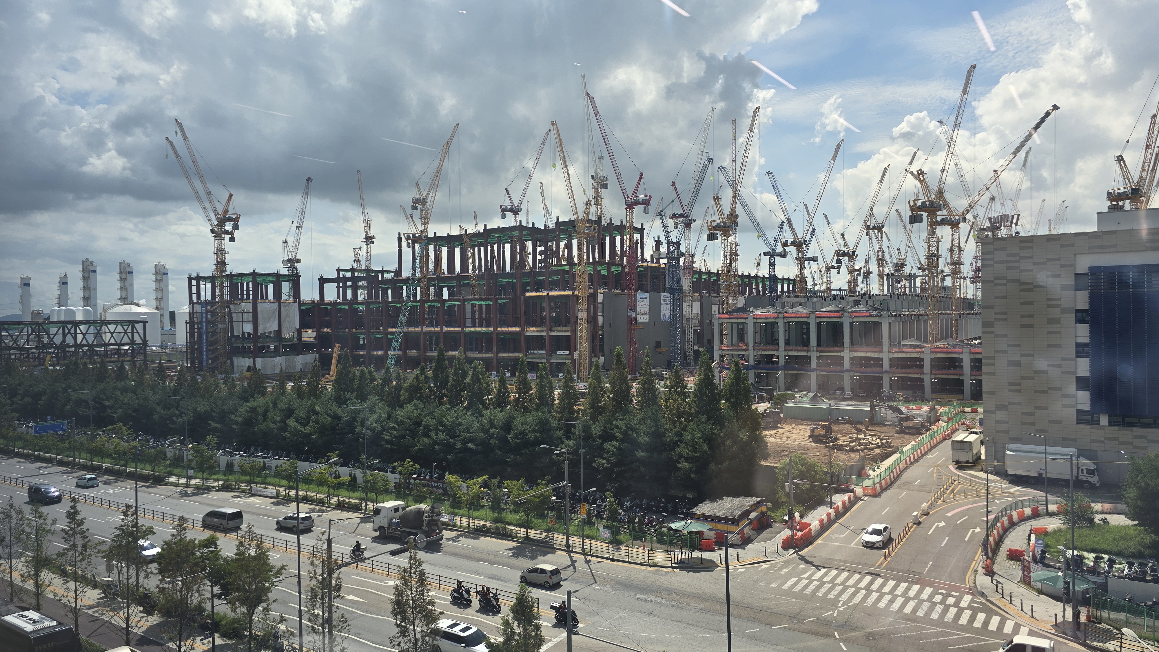
Samsung Electronics’ Pyeongtaek semiconductor campus is more than a collection of large factories. It is a continuously expanding manufacturing ecosystem in which building construction, utility infrastructure, cleanroom installation, semiconductor equipment move-in and production ramp-up take place almost simultaneously.

For the semiconductor equipment industry, understanding this structure is important. A modern fab requires far more than lithography, deposition and etching tools. Behind every wafer process is an enormous supporting network of vacuum pumps, chillers, scrubbers, traps, gas and chemical systems, electrical infrastructure, HVAC systems and process cooling equipment.
As of August 2026, Samsung’s Pyeongtaek campus is moving from the P1–P4 generation into the much larger P5 and P6 expansion cycle, driven increasingly by AI, HBM and advanced memory demand.
Pyeongtaek: From P1 to P6
| Fab | Status | Key Role / Direction |
|---|---|---|
| P1 | Operating | One of Samsung’s first large-scale Pyeongtaek production fabs, initially centered on advanced memory including V-NAND. |
| P2 | Operating | Expanded Pyeongtaek into DRAM, NAND and foundry production using 300mm wafers. |
| P3 | Operating | A major advanced-memory production facility. Industry field observations associate P3 strongly with HBM-related production, although an exclusive Nvidia-only designation has not been publicly confirmed by Samsung. |
| P4 | Partially operating / final build-out | Production is being brought online sequentially as individual cleanroom sections and equipment installations are completed. |
| P5 | Under construction | Targeted for operation from 2028. P5 introduces Samsung’s new “triple-fab” structure and is expected to support HBM, DRAM, NAND and advanced foundry capacity. |
| P6 / P5-2 | Construction accelerated | Planned as an integrated expansion next to P5, with production currently expected around 2029. |
The enormous physical scale of these factories is itself significant. Field observations describe individual Pyeongtaek fab buildings as being on the order of several hundred meters wide and roughly 600 meters long. Newer projects vary in exact dimensions, but each fab represents an industrial complex in its own right.
A Semiconductor Fab Is Really Two Factories in One
What visitors see from outside is only the production building. Under and around the cleanroom is another factory dedicated to keeping semiconductor tools alive.
The lower infrastructure or “sub-fab” areas contain equipment such as:
- Dry vacuum pumps
- Process chillers and cooling systems
- Scrubbers and exhaust abatement systems
- Particle and chemical traps
- Gas and chemical supply infrastructure
- Electrical power distribution
- Process water and cooling-water systems
- HVAC and air-handling systems
Different contractors may use terms such as PCS, PWS or other package-specific terminology for portions of these support systems, but their common function is clear: they provide the stable environment required for the process tools installed in the cleanroom above.
This distinction is also important when discussing the number of “floors.” A fab may physically contain utility, sub-fab and production levels, while the industry term double fab or triple fab normally refers to the number of vertically stacked cleanroom production levels. Public reports describe P1 through P4 as double-fab designs, while P5 is the first Pyeongtaek facility designed around a triple-fab concept.
Why Vacuum Pumps, Scrubbers and Traps Matter More Than Ever
Semiconductor manufacturing consumes enormous amounts of electricity, and equipment suppliers are therefore being pushed toward lower-power solutions.
Vacuum pumps are one important example. Dry vacuum pumps operate continuously on many deposition, etch and other process tools, meaning that even relatively small improvements in pump efficiency can translate into large energy savings across thousands of process chambers.
However, reducing power consumption does not eliminate the exhaust problem. Semiconductor processes generate particles, corrosive gases and chemical by-products that must be safely controlled before exhaust gases can leave the process system.
This creates continuing demand for specialized traps, scrubbers and point-of-use abatement systems working together with the vacuum pump.
The result is an important change in the equipment market: future fab infrastructure will be judged not only by process performance, but increasingly by energy consumption, exhaust management, uptime and total cost of ownership.
300mm Wafers Remain the Core Manufacturing Platform
Samsung’s leading semiconductor fabs are based primarily on 12-inch, or 300mm, wafers.
The advantage of the larger wafer is straightforward: more semiconductor dies can be produced from each wafer, lowering manufacturing cost per chip when yields are properly controlled.
For advanced DRAM, NAND, HBM-related logic and foundry production, the 300mm platform has therefore become the fundamental manufacturing infrastructure.
How a Samsung Fab Is Actually Built
Large semiconductor fabs are not completed first and filled with equipment later. Construction and production preparation overlap.
Samsung C&T has played a major role in construction of Samsung’s Pyeongtaek facilities. Industry field discussions describe the construction-management approach as a form of 5D digital construction planning, in which the physical design is combined with construction sequence, schedule and cost information.
A simplified fab build sequence looks like this:
- Civil and structural construction
- Electrical, piping, utility and HVAC infrastructure
- Cleanroom and sub-fab completion
- Process equipment move-in
- Gas, chemical, vacuum, exhaust and cooling hook-up
- Equipment qualification
- Wafer input and phased production ramp
This explains why a semiconductor fab can be described as “under construction” and “in production” at the same time.
P4 is a good example. Rather than waiting for the entire building to be completed, Samsung is bringing individual sections into operation as construction, equipment installation and qualification are completed.
This phased approach can shorten the time between capital investment and actual semiconductor output — an increasingly important competitive advantage during the current AI-driven memory shortage.
HBM Changes the Relationship Between Memory and Foundry
HBM is no longer simply a DRAM product.
A modern HBM package combines multiple vertically stacked DRAM dies with a sophisticated base die and advanced packaging technologies. Current Samsung HBM products include 8-high and 12-high configurations, while HBM4 uses Samsung’s advanced 1c DRAM together with a 4nm base die.
The base die is particularly important because it connects memory technology with foundry manufacturing. Samsung’s ability to produce memory dies, manufacture advanced logic base dies through its foundry operation and complete advanced packaging gives the company an unusually broad semiconductor manufacturing structure.
After front-end wafer fabrication, Samsung’s Cheonan campus plays a major role in HBM back-end processing and advanced packaging. Samsung is also expanding HBM-related capacity in the Cheonan and Onyang region.
From 8-High and 12-High HBM to zHBM
The next stage may move beyond simply adding more DRAM dies to an HBM stack.
At FMS 2026, Samsung introduced zHBM, a next-generation 3D memory architecture designed to place HBM vertically above an AI accelerator rather than beside it.
The objective is to dramatically shorten the physical distance between compute and memory.
Samsung says the architecture could provide up to eight times the performance of HBM5 while improving power efficiency by as much as three times and significantly reducing thermal resistance.
This direction is important because the future competition in AI semiconductors is increasingly about the entire physical system — logic, memory, interconnect, packaging, cooling and power — rather than the performance of an individual chip.
Beyond Pyeongtaek: Yongin and Gwangju
Pyeongtaek is only one stage of Samsung’s long-term Korean semiconductor expansion.
Samsung plans to build six fabs in the Yongin national semiconductor complex. The first fab is currently targeted to begin operation around 2029, with the overall six-fab development extending toward 2040.
At the same time, Samsung has announced a plan to invest approximately KRW 400 trillion to develop a new semiconductor cluster in Gwangju, including two new semiconductor fabs.
This means Korea could eventually develop three major generations of Samsung semiconductor manufacturing infrastructure:
- Existing semiconductor bases: Giheung and Hwaseong
- Current mega-campus: Pyeongtaek P1–P6
- Next-generation expansion: Yongin and Gwangju
DATAAD View: The Fab Infrastructure Market Is Becoming as Strategic as the Chip
The semiconductor industry is usually discussed in terms of nanometers, EUV, DRAM density or HBM bandwidth.
But a semiconductor factory cannot operate without thousands of pieces of infrastructure equipment working continuously beneath the cleanroom.
Vacuum pumps, chillers, scrubbers, traps, valves, piping, process cooling, chemical distribution, exhaust systems and monitoring equipment are becoming increasingly strategic as fabs grow larger and energy-efficiency requirements become more demanding.
Samsung’s simultaneous expansion in Pyeongtaek, Yongin, Cheonan/Onyang and Gwangju therefore represents more than additional semiconductor capacity.
It creates a long-term industrial market for Korea’s semiconductor equipment and component suppliers.
In the AI era, the winner may not simply be the company that designs the fastest memory chip. It may be the company — and the industrial ecosystem around it — that can build, connect, cool, evacuate, clean, qualify and ramp an entire semiconductor fab faster than anyone else.
DATAAD Research Note — based on industry field observations from August 2026 together with publicly available Samsung Electronics disclosures and Korean semiconductor industry reporting. Fab schedules and product allocations may change according to market conditions and Samsung Electronics’ investment decisions.