The semiconductor industry is entering a new phase in which making smaller transistors is no longer enough.
For decades, the industry's central question was relatively simple:
How small can we make the transistor?
That question still matters.
But AI, high-bandwidth memory, chiplets and heterogeneous integration are adding a much larger set of engineering problems.
How precisely can a wafer temperature be controlled?
How can increasingly deep structures be etched?
How can thousands of process steps be automated?
How can expensive dies be assembled into very large packages without destroying yield?
Can organic substrates continue scaling?
And once multiple high-power dies and HBM stacks are placed inside one package, how should the package itself be cooled?
These questions point toward an important transition:
The semiconductor industry is moving from transistor scaling toward complete system manufacturing.
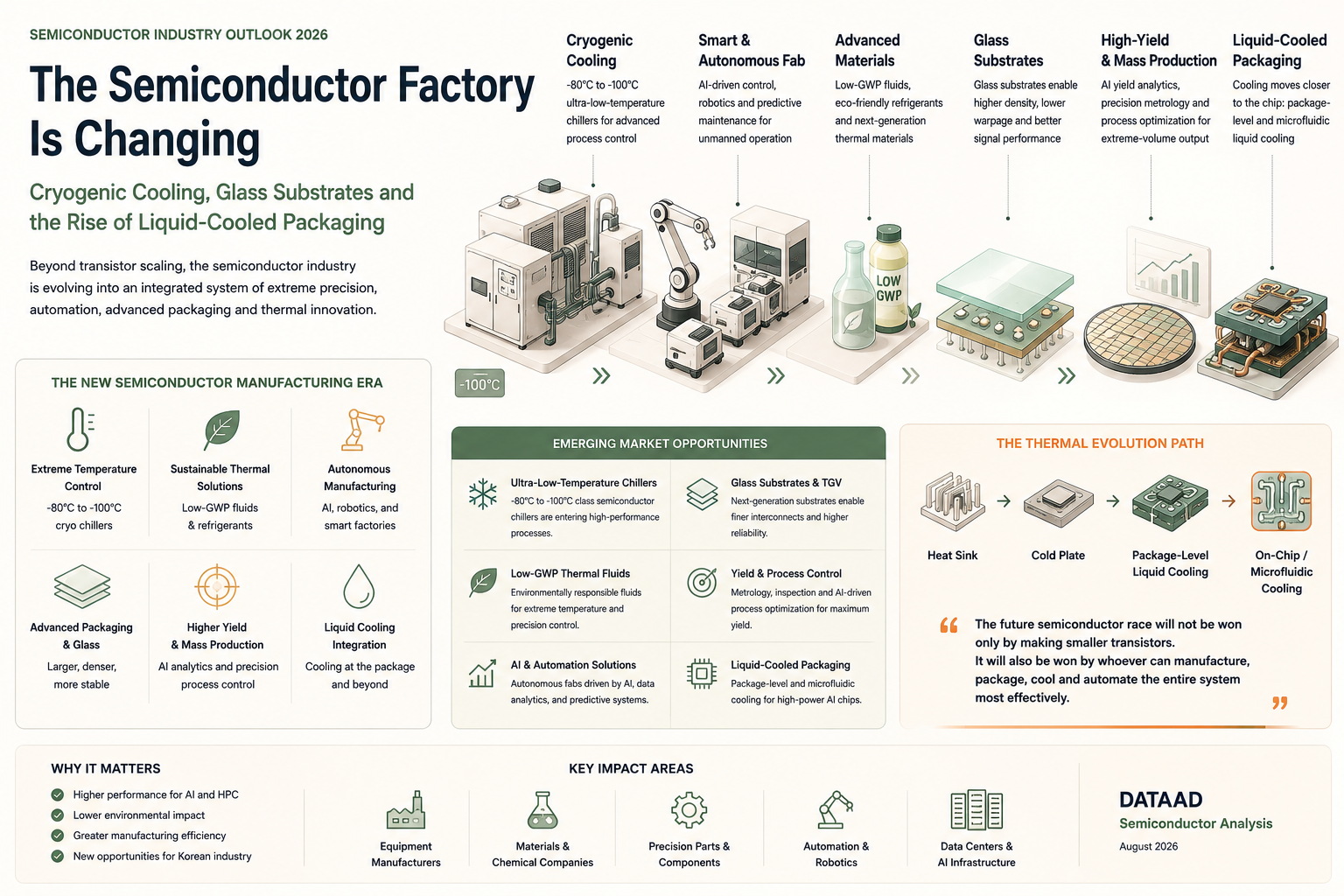
DATAAD sees at least six technology shifts becoming increasingly important:
- Ultra-low-temperature semiconductor chillers
- Low-GWP refrigerants and thermal fluids
- AI-driven and increasingly autonomous semiconductor manufacturing
- Glass substrates for advanced packaging
- Yield optimization for extremely high-volume advanced packaging
- Liquid cooling moving closer to — and eventually into — the semiconductor package
1. Semiconductor Cooling Is Moving Toward -80°C and -100°C
One of the less visible changes in semiconductor manufacturing is happening below zero.
Temperature-control requirements for advanced semiconductor equipment are becoming increasingly demanding, particularly in etch and other precision processes.
This does not mean every semiconductor tool will operate at -100°C.
But an increasing class of equipment is being developed specifically for ultra-low-temperature process control.
Korean semiconductor-equipment company UNISEM, for example, lists its RUCS30000Z ultra-low-temperature chiller with a temperature range from -100°C to +20°C, including approximately 2 kW of cooling capacity at -100°C.
GST also lists cryogenic semiconductor chillers supporting the -80°C class, including an RSHD platform rated at approximately 10 kW at -80°C under specified operating conditions.
This change is closely connected to changes occurring inside the process chamber.
Lam Research's Cryo 3.0 technology is designed for cryogenic dielectric etching in advanced 3D NAND manufacturing. Lam says cryogenic etch entered volume production in 2019 and that nearly 1,000 of more than 7,500 Lam high-aspect-ratio dielectric etch chambers in NAND production were using cryogenic technology when Cryo 3.0 was announced.
As memory structures become deeper and more complicated, temperature is increasingly another process parameter that must be controlled with extreme precision.
The semiconductor chiller is becoming process equipment, not simply utility equipment.
2. The Thermal Fluid Is Becoming Strategically Important
Moving toward extreme temperatures creates another challenge.
The circulating fluid itself must continue to perform.
Viscosity changes.
Freezing point matters.
Material compatibility matters.
Electrical insulation can matter.
And environmental regulation is becoming increasingly important.
Daikin's DAISAVE portfolio illustrates this transition. The company specifically identifies semiconductor processes including etching, film deposition and ion implantation as applications requiring increasingly precise temperature control across very wide temperature ranges.
Its SS-110 fluorinated heat-transfer fluid, designed for semiconductor chillers, has a listed freezing point below -130°C and GWP below 100. Daikin also lists applications including electrostatic-chuck temperature control for dry etching, lithography light-source temperature control and ion implantation.
This is an important market signal.
Future semiconductor cooling will not be defined only by the chiller.
It will increasingly be defined by:
Chiller + Refrigerant + Secondary Fluid + Hose + Seal + Connector + Process Chamber
3. Low-GWP Cooling Is Becoming Part of Semiconductor Equipment Design
The semiconductor industry faces another transition at the same time: reducing dependence on high-GWP fluorinated refrigerants and process fluids.
There are several possible paths, and they should not be confused with one another.
A chiller may use a low-GWP refrigerant while circulating a separate heat-transfer fluid.
A process loop may use a low-GWP fluorinated thermal fluid.
And future two-phase thermal systems may use another working-fluid architecture entirely.
For example, SMC has introduced semiconductor thermo-chillers using R744 CO₂ refrigerant with GWP 1.
GST also lists a semiconductor chiller using R744 CO₂ as the refrigerant, demonstrating that this environmental transition is already reaching Korean semiconductor-equipment suppliers.
Meanwhile, Daikin is developing low-GWP fluorinated liquids for heat-transfer applications.
The next step could become even more interesting.
As semiconductor and AI thermal densities rise, engineers are also studying phase-change and two-phase cooling, where thermal energy is transported through evaporation and condensation rather than only through sensible heating of a liquid.
This should still be considered an emerging technology rather than a universal semiconductor-industry standard.
But if it expands, fluid selection will become a strategic part of semiconductor thermal architecture.
4. The Fab Is Becoming More Autonomous
At the same time that process temperatures become more extreme, semiconductor manufacturing is moving toward greater automation.
Modern fabs already use extensive automated material handling.
The next step is deeper automation of the manufacturing decisions themselves.
SEMI's 2026 AI Techniques in Semiconductor Manufacturing program highlights the industry's movement toward AI-supported yield management, fault detection and classification, run-to-run control, design of experiments and increasingly autonomous analytical workflows.
The direction is significant.
The future semiconductor factory may increasingly combine:
Automated Material Handling
+
Equipment Sensors
+
Process Data
+
AI Yield Analysis
+
Automated Recipe Optimization
+
Predictive Maintenance
SEMI's 2026 Intelligent Manufacturing Showcase described AI, automation, digitalization and human-machine collaboration as technologies already shaping high-volume semiconductor fabs rather than concepts belonging only to the future.
The fab is gradually becoming a physical AI system.
5. The Goal Is Not Automation for Its Own Sake — It Is Yield
A semiconductor factory does not make money simply because it is automated.
It makes money when more good chips emerge from the same manufacturing capacity.
This makes yield one of the most important economic variables in the semiconductor industry.
Advanced packaging makes this problem even more important.
Imagine assembling several expensive compute dies, HBM stacks, interposers and substrates into one package.
A defect late in the process can destroy the value already accumulated in all of those components.
This changes the economic equation.
As package value rises, the cost of every manufacturing defect rises with it.
This is why AI-enabled process control, inspection, metrology and yield management are becoming increasingly strategic.
SEMI's 2026 advanced-packaging discussions specifically highlighted metrology and inspection capabilities required for high-yield manufacturing as advanced packaging expands for AI and high-performance computing.
6. AI Is Driving Semiconductor Manufacturing Toward Extreme Volume
The problem is not only yield.
The industry also has to achieve that yield at enormous scale.
AI infrastructure requires huge quantities of:
- GPU and accelerator dies
- HBM
- Advanced substrates
- Interposers
- Chiplets
- Packaging materials
- Power-delivery components
This pushes advanced packaging from a specialized high-end process toward something closer to industrial mass production.
Intel's advanced-packaging facilities provide one illustration. The company says its current technology can build packages approximately eight times the standard reticle scale, with a roadmap toward more than 12 times by 2028.
This is a fundamental change.
The semiconductor package is no longer merely the protective shell around one chip.
It is becoming a platform that integrates many chips into one computing system.
7. Glass Substrates Could Change the Foundation of the Package
As packages become larger and denser, conventional organic substrates face increasing physical challenges.
This is why glass is receiving serious attention.
Intel has been developing glass substrates for next-generation advanced packaging and says glass can support significantly improved design rules, higher interconnect density, improved dimensional stability and large package sizes for future data-center and AI applications.
In July 2026, Intel also announced a collaboration with Lens Technology focused on precision glass processing for future advanced semiconductor packaging.
Glass can offer several attractive characteristics:
- Lower warpage for large packages
- Better dimensional stability
- Fine-pitch interconnect potential
- Through-glass vias
- Improved high-frequency electrical characteristics
- Potential optical integration
Intel has described glass as an important potential foundation for future AI and HPC heterogeneous integration.
This means a future advanced package might evolve from:
Organic Substrate + Single Die
toward:
Glass Substrate + Multiple Chiplets + HBM + Advanced Power Delivery + Optical I/O
8. Packaging Is Becoming Part of the Computer Architecture
Advanced packaging was once considered a back-end step that followed chip manufacturing.
That distinction is disappearing.
Intel describes advanced packaging as essential for connecting specialized chiplets so that they function as one powerful system.
TSMC's CoWoS and other heterogeneous-integration platforms follow the same broad direction.
The package increasingly determines:
- Memory bandwidth
- Chip-to-chip bandwidth
- Power delivery
- Signal integrity
- Package size
- Thermal performance
So the future semiconductor competition is not simply:
Who has the smallest transistor?
It increasingly includes:
Who can build the best system of chips?
9. And Now Cooling Is Moving Into the Package
This is where semiconductor manufacturing begins to overlap directly with liquid cooling.
Traditional thermal architecture places a thermal interface material and heat sink or cold plate above the finished package.
As package power rises, engineers are exploring ways to bring liquid much closer to the silicon.
TSMC research has demonstrated advanced liquid cooling on CoWoS packages at thermal design powers up to approximately 2 kW.
TSMC has also demonstrated direct silicon water cooling using a bonded silicon lid with cooling structures, reporting heat removal above 2,600 W from a single SoC in research.
Imec has similarly demonstrated silicon microchannel and direct-impingement approaches that move coolant much closer to the chip.
This suggests a long-term thermal progression:
Heat Sink → Cold Plate → Package-Level Liquid Cooling → On-Chip / Microfluidic Cooling
This does not mean every semiconductor package will soon contain coolant channels.
These remain advanced technologies.
But the direction matters.
Cooling is moving from the data center toward the rack.
From the rack toward the server.
From the server toward the package.
And eventually, potentially, toward the silicon itself.
10. Semiconductor and Data Center Cooling Are Beginning to Converge
Historically, semiconductor manufacturing cooling and data-center cooling were different industries.
A semiconductor fab used process chillers to precisely control manufacturing equipment.
A data center used HVAC systems to cool finished computers.
AI is beginning to connect them.
The same industrial disciplines are increasingly relevant to both:
- Advanced heat-transfer fluids
- Low-GWP refrigerants
- Pumps
- Heat exchangers
- Quick disconnects
- Hoses
- Seals
- Flow control
- Leak detection
- Precision thermal management
This convergence creates an interesting new market.
The semiconductor industry makes the AI chip.
The cooling industry makes it possible to manufacture — and operate — that chip.
11. Korea Could Be Particularly Interesting in This Transition
Korea has obvious strengths in semiconductor memory and manufacturing.
But the next semiconductor cycle may create opportunities much further down the supply chain.
Korean companies already have commercial experience in ultra-low-temperature semiconductor chillers.
UNISEM lists a -100°C-class semiconductor chiller, while GST markets cryogenic chillers and is also developing environmentally focused thermal systems.
Fine Semitech has spent decades developing semiconductor chillers and temperature-control equipment.
The broader Korean industrial base also includes:
Precision Machining + Pumps + Valves + QDs + Hoses + Thermal Materials + HVAC + Automation + Robotics
That becomes increasingly important if semiconductor manufacturing moves toward:
Extreme Temperature + Extreme Precision + Extreme Automation + Extreme Packaging Density.
12. The Next Semiconductor Equipment Market May Look Very Different
The traditional semiconductor equipment industry concentrated around deposition, lithography, etching, cleaning and inspection.
Those technologies remain essential.
But another equipment layer is growing around them.
| Technology Shift | New Requirement |
|---|---|
| Cryogenic Processing | -80°C to -100°C-class precision thermal control |
| Environmental Regulation | Lower-GWP refrigerants and process fluids |
| Autonomous Manufacturing | AI, sensors, robotics and predictive maintenance |
| Higher Yield | Metrology, inspection and process analytics |
| Advanced Packaging | Large-area and high-precision manufacturing |
| Glass Substrates | TGV, precision glass processing and new equipment |
| High-Power AI Packages | Package-integrated and microfluidic cooling |
13. DATAAD Outlook: The Semiconductor Factory Becomes a Physical AI Factory
The next semiconductor factory will still contain lithography machines, etchers and deposition tools.
But around them will be another increasingly sophisticated layer.
Ultra-low-temperature chillers.
Low-GWP fluids.
AI process control.
Robotic material handling.
Predictive maintenance.
Advanced inspection.
Glass-substrate processing.
High-volume heterogeneous packaging.
And eventually, liquid cooling integrated much closer to the package itself.
The progression can be summarized simply:
Smaller Transistor → More Chips per Package → More Heat → More Manufacturing Complexity → More Automation
The semiconductor factory therefore becomes much more than a place where wafers are processed.
It becomes an integrated system of:
Materials + Equipment + Data + AI + Robotics + Thermal Engineering
That is effectively a form of Physical AI.
14. DATAAD Insight
The semiconductor industry's next transformation may not be defined by a single breakthrough.
It may come from several technologies arriving at the same time.
-100°C-class thermal control.
Low-GWP cooling.
Autonomous manufacturing.
Glass substrates.
Higher packaging yield.
Extreme-volume production.
Package-integrated liquid cooling.
Each looks like a separate technical market.
In reality, they are increasingly connected.
The future semiconductor race will not be won only by making smaller transistors.
It will also be won by whoever can manufacture, package, cool and automate the entire system most effectively.
And that could create a much broader semiconductor opportunity for equipment companies, materials companies and precision manufacturers than the industry has seen before.
Editorial Note
This article distinguishes between technologies already in high-volume production and technologies that remain in development.
Cryogenic semiconductor processing and ultra-low-temperature chillers already exist commercially. Glass substrates, package-integrated cooling and deeper microfluidic cooling are at different stages of research, development and commercialization and should not be interpreted as universal near-term industry standards.
Likewise, low-GWP refrigerants, low-GWP heat-transfer liquids and two-phase working fluids are technically different categories and should not be treated as interchangeable.
DATAAD Semiconductor Analysis · August 2026
Primary source basis includes official materials from Lam Research, Intel, TSMC, imec, SEMI, Daikin, SMC, UNISEM, GST and Fine Semitech.